
Stamp Holes in PCB Fabrication: Design Standards, Applications, and Panelization Techniques
Release time:
2025-07-17

Stamp Holes
PCB stamp holes are a method used on board edges or during panelization to facilitate board separation. In a main panel layout, small boards need to be connected by connecting strips. To make cutting easier, small holes are drilled into these strips—similar to the perforations on the edges of stamps—and these holes are called stamp holes.
Continued:
1.Suitable for boards with high 外形要求 (milling for board separation).
2.Stamp holes can avoid positions where components are placed on the board edge; there should be no pads or through-holes within a 1mm range of stamp holes.
3.Applicable to scenarios where Layout is restricted and components on the board edge need to be avoided.
Types of Stamp Holes
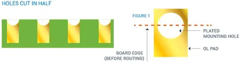
1.Half-holes
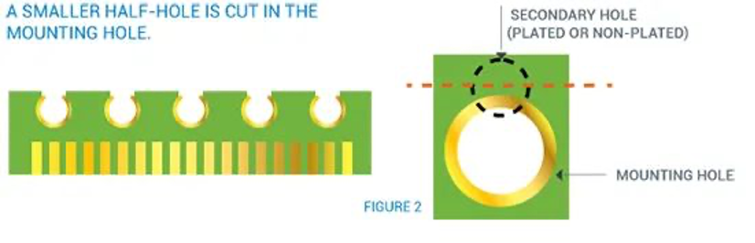
 2.Half-holes with smaller diameters
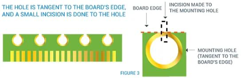
 3.Holes tangent to the board edge
Standard Spacing for Stamp Holes
Stamp holes are typically non-metallized holes (NPTH) with a diameter of 1.0mm (40mil), spaced at 1.27mm (50mil) center-to-center, and recessed 0.4mm (16mil) from the main PCB edge.
Functions of Stamp Holes
While most PCBs use V-CUT for panelization, stamp holes are employed for:
1.Irregular or circular PCB shapes where V-CUT is impractical.
2.Supporting panelized boards during manufacturing to prevent separation before depanelization.
3.Maintaining mold integrity during PCB fabrication (prevents mold collapse).
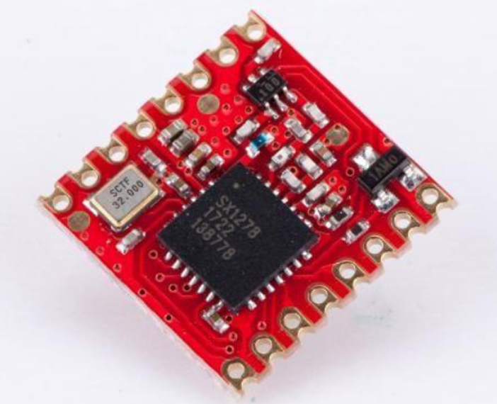
Common applications include creating modular PCBs (e.g., Wi-Fi modules, Bluetooth boards, or core processor modules) that are later assembled onto a larger PCB as discrete components.
Key Terminology Notes
*Non-metallized holes (NPTH): Critical for avoiding electrical connections between panels.
*Recessed from the edge: Ensures structural integrity while allowing clean separation.
*Panelization: The process of arranging multiple PCBs on a single panel for efficient manufacturing.


Lihai Industrial Park, Baohuan Middle Road, Shatian Town, Dongguan , China.
Room 2314-2315, Zhonghui IFC Nansha District, Guangzhou.
Online Message
Copyright 2024 © Guangzhou Leizzi Electronic Technology Co., Ltd. All Rights reserved.